About Me
Settings Optimization intern at Formlabs, working in a mixed lab + data focused test and development space. Workflow involves Git based source management, Python for json scripting and data analysis, SOP documentation, metrology for mechanical and optical properties.
My work involves discussions around product development, shipping, and stakeholder meetings. Methodologies such as: Design for Manufacturing (DFM), Design for Test (DFT), Rapid Prototyping (RP)
Director for UW-NanoRobotics Group, advancing additive manufacturing for flexible electronics. We also host an endorsed and accredited curriculum program with the Waterloo Institute of Nanotechnology (WIN) to reinforce engineering concepts through hands-on projects.
4 Fun
Climbing, and when I'm lucky kitesurfing are my favourite ways to spend time, I'm also a big fan of cooking and trying new recipes.
Patents and Publications
Photoanode Deposition Process Design (Patent Pending)
- Developed a deposition process for MANTECH's COD biosensors to achieve desired thickness and porosity
- Resolved yield issues by adjusting deposition parameters and implementing new data acquisition and QA steps
- Created SOPs and instructional videos to ensure the deposition process can be replicated for device production.
Laser Induced Defect TiO2 for Solar Panels and Water Sensing (Publication Pending)
- Fabricated photocatalytic cells to be applied to solar conversion and wastewater sensing
- Optimized deposition techniques for anode materials with Python & data analysis principles
- Ensured feasibility of research-oriented process design for industrial use and scalability
UW-NanoRobotics Group
Director for the University of Waterloo NanoRobotics Group
- Originally the materials team lead, where we made conductive inks. More on that...
- Leading 70+ students across engineering, science, and business to advance additive manufacturing
- Established an accredited, endorsed curriculum program with the Waterloo Institute of Nanotechnology (WIN) to reinforce engineering concepts through hands-on projects
Conductive Ink Synthesis and R&D for Additive Manufacturing (In Progess)
- Directed synthesis of silver nanoparticles for use in flexible PCBs with an application to wearable electronics
- Tested ink conductivity, adhesion, and ductility with various substrates and sintering temperatures
- Collaborated through goal alignment and technical documentation including SOPs and BOMs
Experience
Nano & Micro Systems Lab
Research Assistant
- Assisted in the fabrication of micro-scale devices using cleanroom protocols.
- Conducted material characterization using SEM and optical microscopy.
- Optimized etching processes for silicon-based substrates.
Nano & Micro Systems Lab
Research Assistant
- Advanced thin-film deposition techniques for functional nanomaterials.
- Analyzed experimental data to correlate process parameters with device performance.
- Collaborated on publication-quality technical documentation and lab reports.
Formlabs
Settings Optimization Intern
- Automated data analysis pipelines using Python for resin printing performance.
- Managed Git-based source control for JSON print-setting configurations.
- Performed metrology on mechanical properties of printed parts for QA validation.
Formlabs
Settings Optimization Intern
- Developed SOPs for new hardware testing and metrology workflows.
- Optimized optical property testing parameters for translucent materials.
- Collaborated with cross-functional teams to align R&D goals with manufacturing needs.
Contact Information
Email: [email protected]
LinkedIn: linkedin.com/in/jericho-mordasiewicz
Nano Silver Conductive Inks
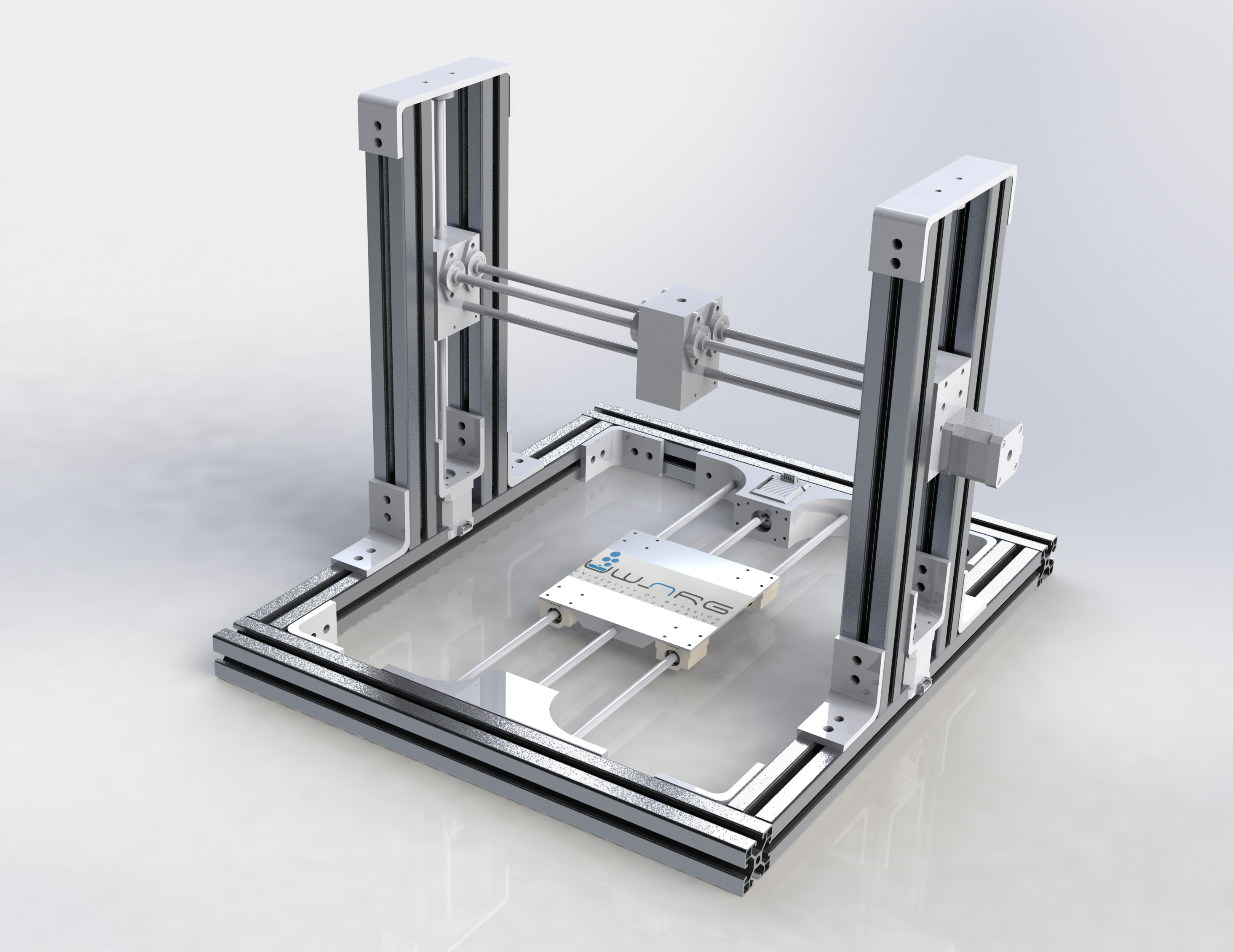
Conductive Hybrid Ink Printer (CHIP)
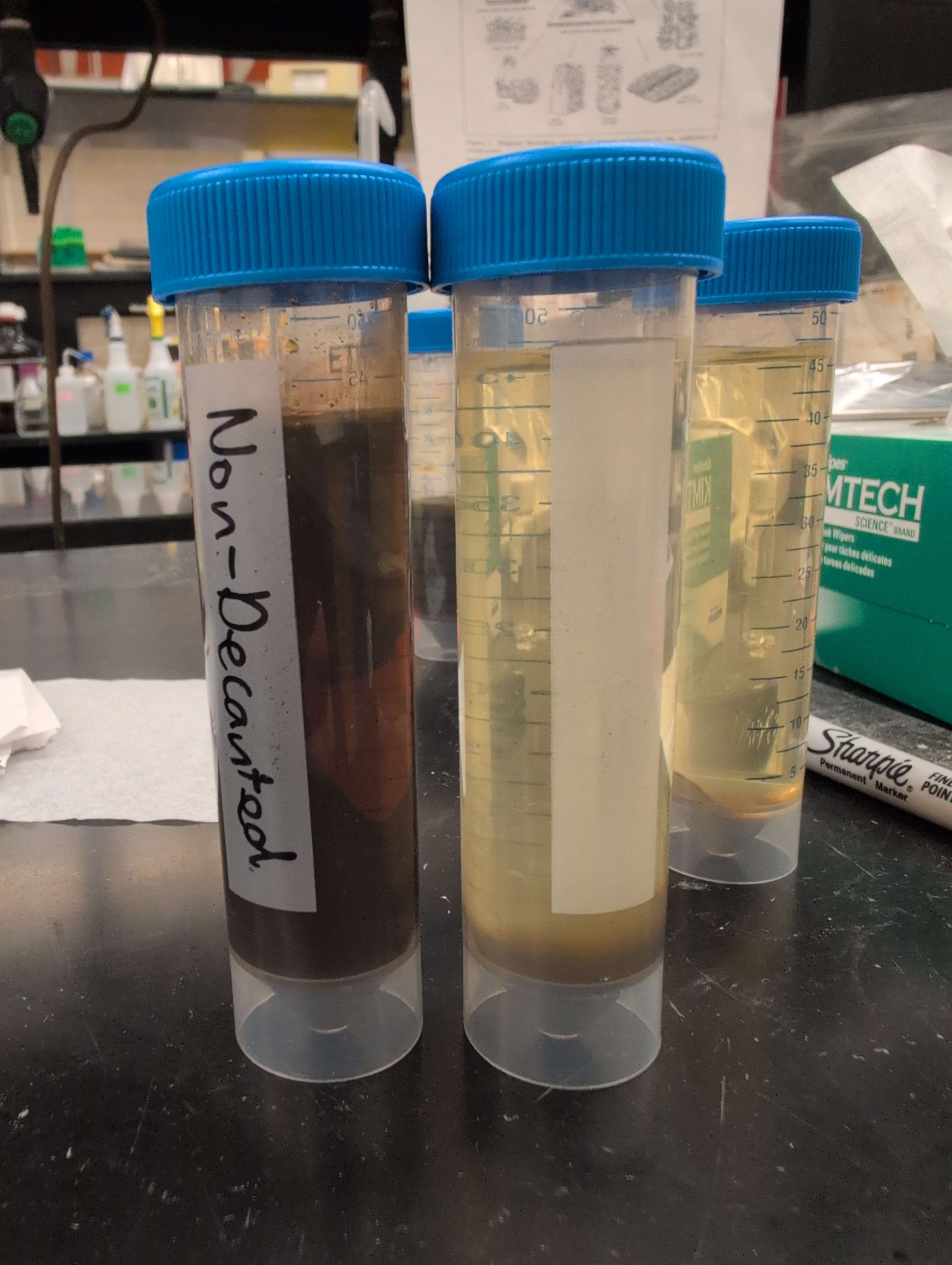
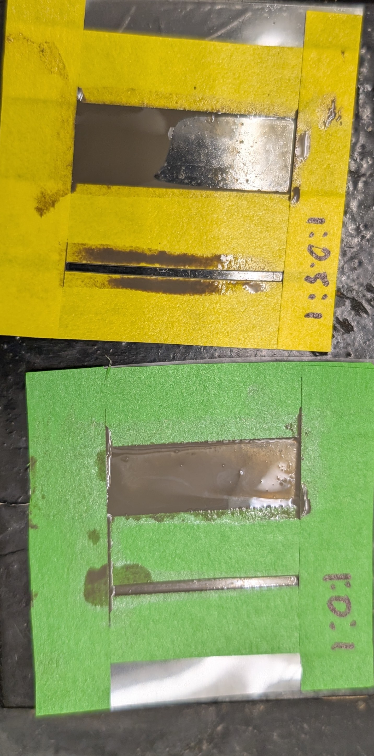
Tested Viscosity Across Different Solvent Ratios
Project Overview
In this project, I led a multidisciplinary team focused on the synthesis and optimization of conductive inks for additive manufacturing, specifically targeting silver nanoparticle formulations for flexible PCBs in wearable electronics. This ink could be used by the printer the mechanical team was designing (CHIP, pictured above). My leadership responsibilities included setting project milestones, aligning team goals, and facilitating R&D, production, and quality assurance (QA). I established clear communication channels and coordinated the creation of technical documentation such as SOPs and BOMs to ensure knowledge transfer and process consistency. By mentoring junior researchers and fostering a collaborative lab environment, I helped drive innovation in ink formulation, deposition techniques, and performance testing, all while maintaining a strong focus on safety and reproducibility.
Technologies Used
- SEM/XRD/DLS for nanoparticle morphology, crystalline structure, and size distribution, respectively.
- Collaborative tools (Git, Notion) for version control and technical documentation
- Python scripts for analyzing conductivity/adhesion test data
- General lab skills and knowledge transfer
- Thermal sintering ovens with programmable temperature profiles
Working On
- Conductivity improvements -> mainly particles diameter control and mass loading
- Viscosity control -> Optimizing binder-to-solvent ratios for printhead compatibility
- Sintering processes -> Literature review and emperical testing
Deposition Process Design
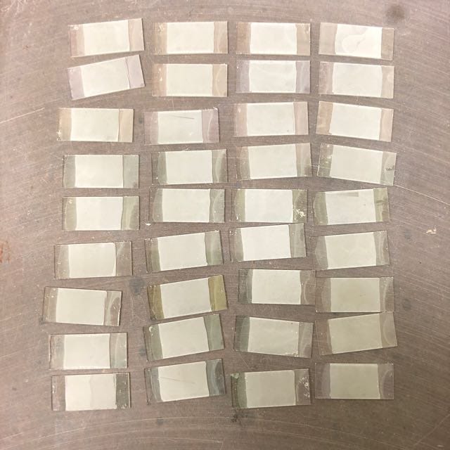
Before Implementation
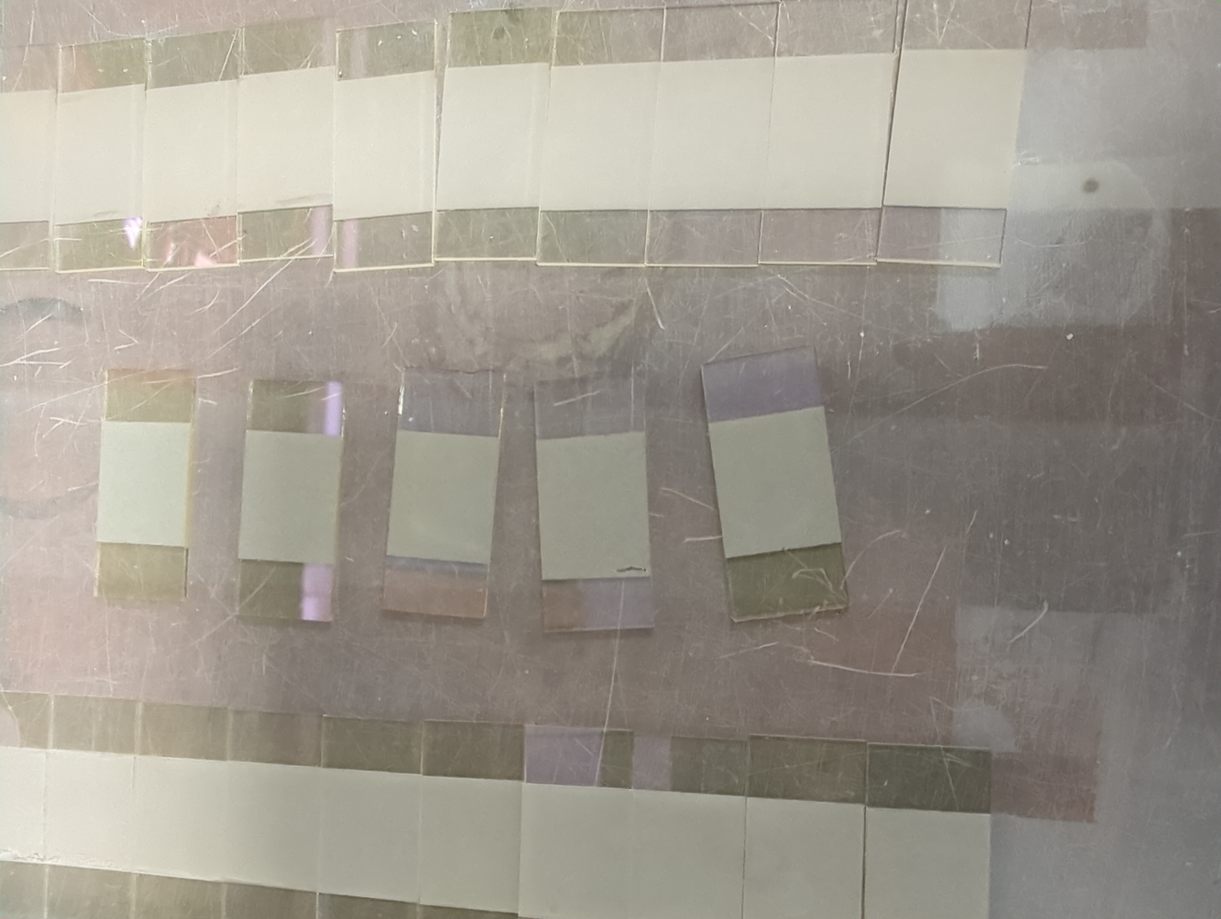
After Implementation
Project Overview
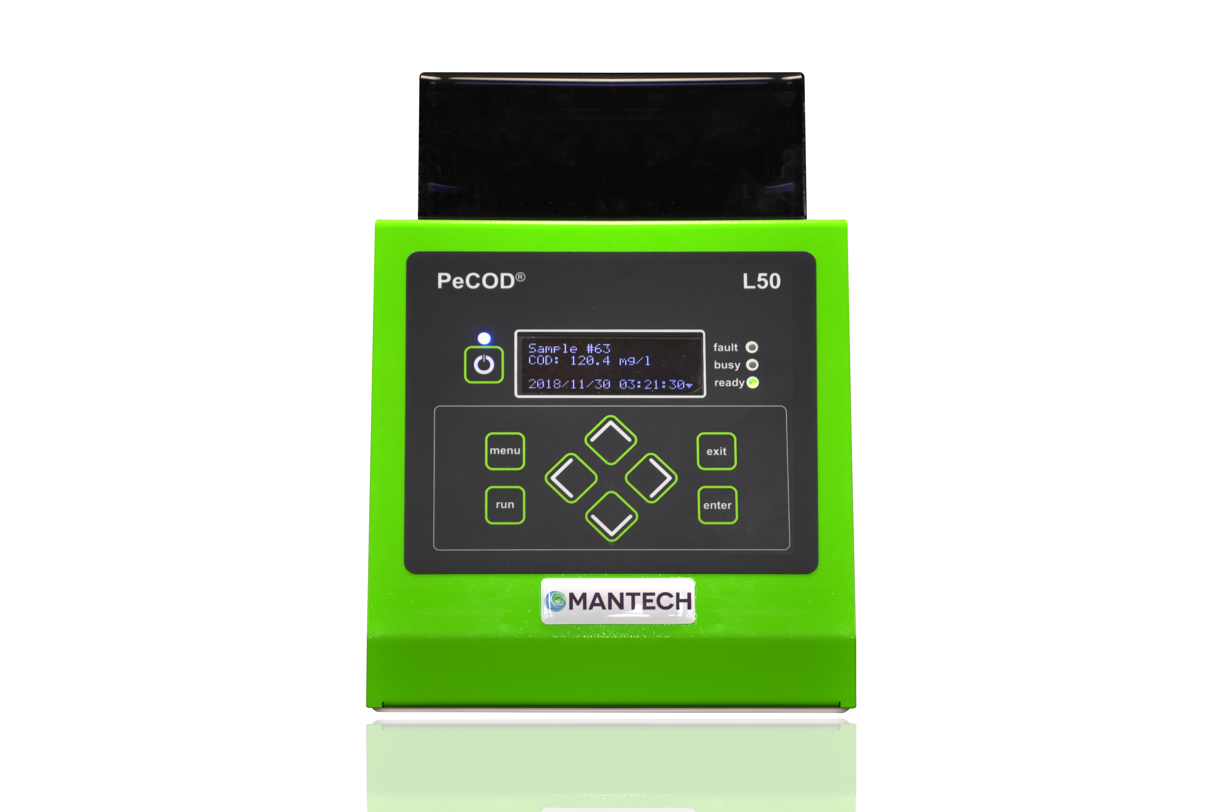
My role was to develop a deposition process for MANTECH’s chemical oxygen demand (COD) biosensors. I wanted to achieve a uniform coating of the photoanode material on the substrate, increase yield, and improve adhesion (therby lifetime of the sensor). My two main focuses were on the environmental factors affecting the deposition process (temperature, humidity) as well as the human error/variability observed bewtween batches. I tuned the solution's surface tension to ensure it could be evenly deposited onto the substrate with the desired thickness and porosity. The initial results were promising but indicated room for improvement in yield and adhesion. To enhance the yield, I adjusted deposition parameters and implemented new quality assurance (QA) steps using data acquisition. The adhesion issues between batches were solved by employing a surface treatment normally used for silicon wafers in the Quantum Nano Fabrication and Characterization Facility (QNFCF) cleanroom. I then created comprehensive standard operating procedures (SOPs) and instructional videos to ensure the process could be consistently replicated for device production.
**I signed an NDA with MANTECH and am unable to share the exact details of the deposition process.**
Technologies Used
- UV-VIS spectroscopy to monitor oxidation of reference pollutants
- Plasma etching to clean and functionalize the surface for wetability (in cleanroom)
- Open source process flow tools to design, test, and ensure QA standards are met
- Python for data aquisition, analysis and process optimization
Results
- Quality assurance (QA) protocols, allowed a 150% increase in device production volume
- Device yield was increased by 15%, manufacturing time reduced by 40%
- Environmental factors no longer have drastic (or any observed) affects on yield
- MANTECH’s in-house average QA runtime was reduced from 6h to 3h due to the film's stable nature
Laser induced Defect TiO2 for Solar Panels and Water Sensing
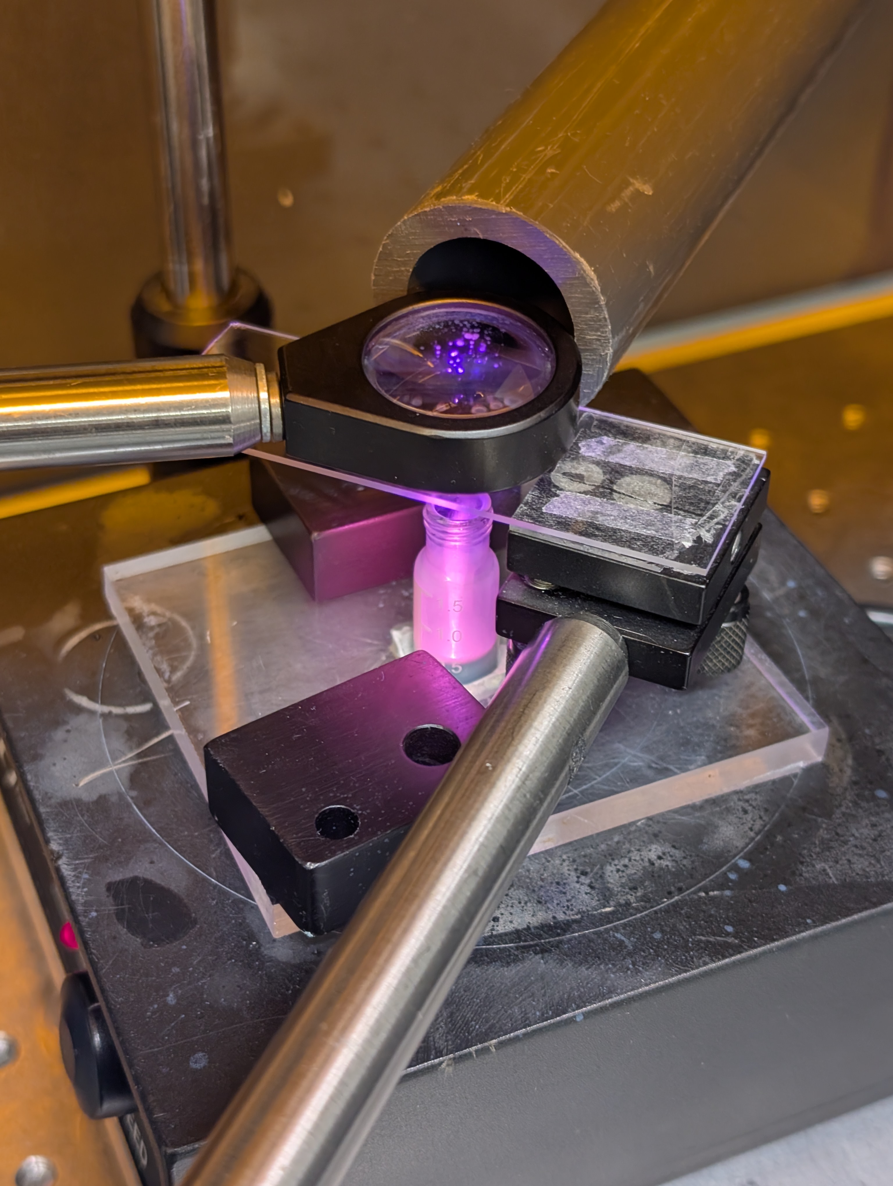
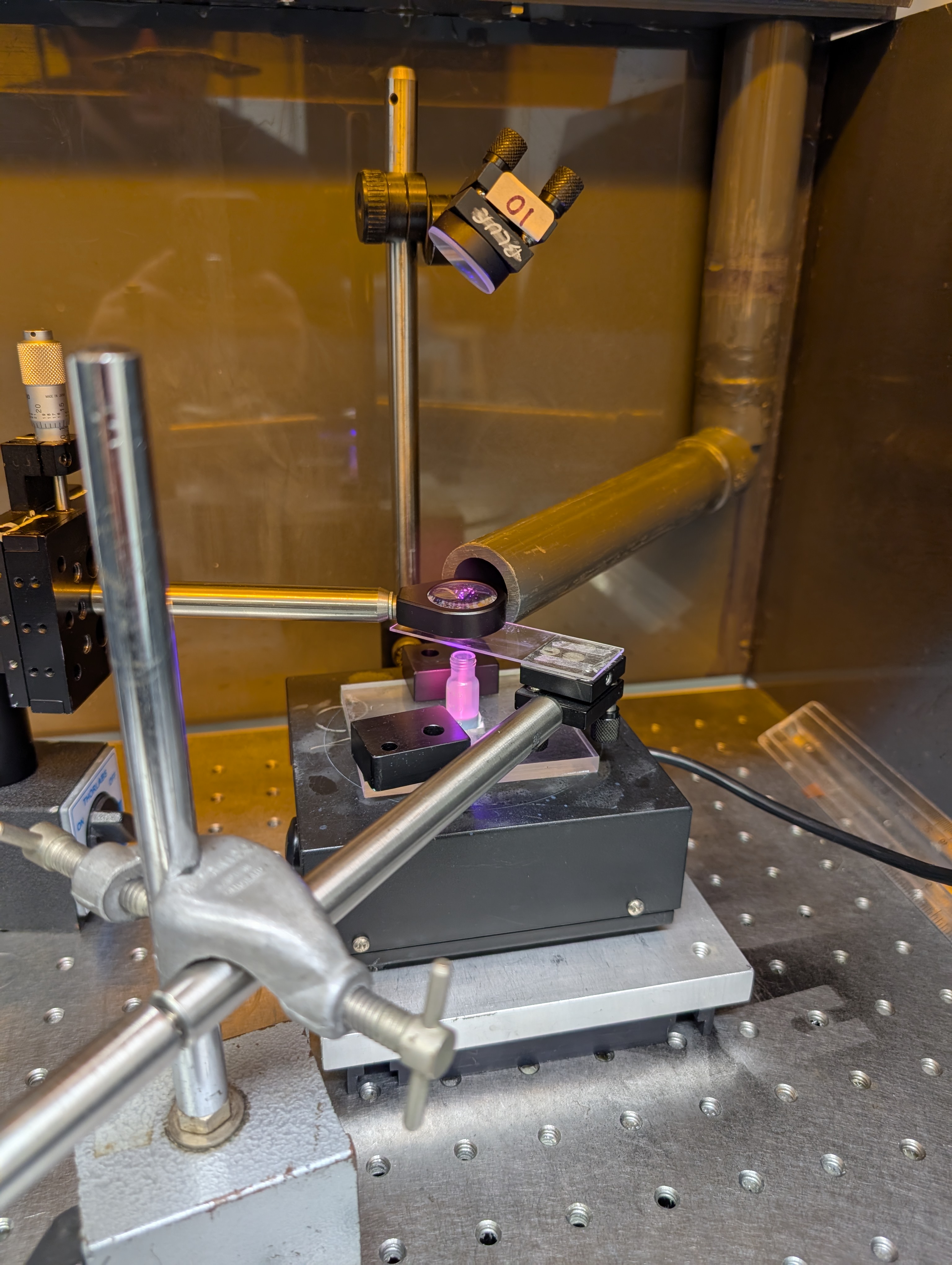
Femtosecond Laser Setup
Photoanode degradation >:(
Project Overview
My role focused on developing laser-induced defect TiO₂ photoanodes for applications in solar energy conversion, organic pollutant oxidation (breaking down harmful chemicals), and wastewater sensing. Key objectives included achieving uniform defect engineering, preventing photoanode degradation, and ensuring reliable fabrication for industrial adoption. Using root cause analysis with cyclic voltammetry (CV) and electrochemical impedance spectroscopy (EIS), I identified and mitigated degradation mechanisms in TiO₂, enabling stable performance. I optimized spray-coating deposition parameters (e.g., material composition, pressure, and surface treatment) to control film quality, nanosecond-pulsed TiO₂ for Ti³⁺/oxygen vacancies, and femtosecond-pulsed TiO₂ for surface-localized Ti³⁺/oxygen vacancies. Batch-to-batch variability was addressed through Python-driven data analysis, which correlated process inputs with material properties. Standardized protocols were then developed to ensure reproducibility across academic and industrial settings.
Technologies Used
- Electrochemical methods: CV, LSV, EIS, for redox couples, (ir)reversible capacitive effects, double layer charging, approximate electrochemical surface area, and solar light
- Nanosecond/femtosecond pulsed lasers to tailor TiO₂ defect profiles
- Spray coating, optimized for 95% throughput with controlled porosity/thickness
- Data acquisition with BioLogic and analysis with Python for quality analysis and control
- Material characterization with SEM, and XRD (not by me) to validate defect states (Ti³⁺, oxygen vacancies), UV-vis for pollutant oxidation behavior
Results
- Eliminated photoanode degradation, enabling the material to be photocatalytically tested
- Achieved 95% throughput in electrode fabrication via spray-coating optimization
- Reduced batch variability by 70%, process design validated for small scale
- Soon to be published :D